Power Electronics In forward blocking mode of a thyristor junction J3 is in forward bias and J1, J2 is in reverse bias. junction J2 is in reverse bias and J1, J3 is in forward bias. Junction J1, J3 is in reverse bias and J2 is in forward bias. Junction J1 and J2 is in forward bias and J3 is in reverse bias. junction J3 is in forward bias and J1, J2 is in reverse bias. junction J2 is in reverse bias and J1, J3 is in forward bias. Junction J1, J3 is in reverse bias and J2 is in forward bias. Junction J1 and J2 is in forward bias and J3 is in reverse bias. ANSWER DOWNLOAD EXAMIANS APP
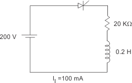
Power Electronics Latching current for an SCR inserted between a dc voltage source of 200 V and load is 100 mA. Compute the minimum rate of width pulse required to turn ON the SCR in case load consists of R = 20 Ω in series with L = 0.2 H. 100 µs. 150 µs. 300 µs. 200 µs. 100 µs. 150 µs. 300 µs. 200 µs. ANSWER DOWNLOAD EXAMIANS APP
Power Electronics Dynamic equalizing circuit is used for equal division of voltage across each thyristor. equal division of current through each thyristor in series. equal division of voltage across each thyristor in parallel. equal division of current through each thyristor in parallel. equal division of voltage across each thyristor. equal division of current through each thyristor in series. equal division of voltage across each thyristor in parallel. equal division of current through each thyristor in parallel. ANSWER DOWNLOAD EXAMIANS APP
Power Electronics A power semiconductor may undergo damage due to Low di/dt. Low dv/dt. High dv/dt. High di/dt. Low di/dt. Low dv/dt. High dv/dt. High di/dt. ANSWER DOWNLOAD EXAMIANS APP
Power Electronics Light triggering mainly used in low - voltage direct current transmission. all of these. high voltage direct current transmission. medium voltage direct current transmission. low - voltage direct current transmission. all of these. high voltage direct current transmission. medium voltage direct current transmission. ANSWER DOWNLOAD EXAMIANS APP
Power Electronics Snubber circuit is used with SCR anti parallel. in parallel. either series or parallel. in series. anti parallel. in parallel. either series or parallel. in series. ANSWER DOWNLOAD EXAMIANS APP