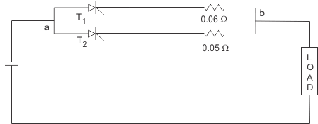
Power Electronics Figure shows two thyristors rated 400 A sharing a load current. Current through T2 is 180A. Current through T1 will be 120 A. 110 A. 100 A. 150 A. 120 A. 110 A. 100 A. 150 A. ANSWER DOWNLOAD EXAMIANS APP
Power Electronics ON state voltage drop across SCR lie between the range 1.5 - 2 V. 1 - 1.5 V. 0 - 0.5 V. 0.5 - 1 V. 1.5 - 2 V. 1 - 1.5 V. 0 - 0.5 V. 0.5 - 1 V. ANSWER DOWNLOAD EXAMIANS APP
Power Electronics To turn on UJT, the forward bias on the emitter diode should be ___________ the peak point voltage. More than Equal to None of these Less than More than Equal to None of these Less than ANSWER DOWNLOAD EXAMIANS APP
Power Electronics A diac is ___________ switch A mechanical A d.c. An c. None of these A mechanical A d.c. An c. None of these ANSWER DOWNLOAD EXAMIANS APP
Power Electronics Which following is a two terminal three layer device? BJT. MOSFET. Power dioed. None of above. BJT. MOSFET. Power dioed. None of above. ANSWER DOWNLOAD EXAMIANS APP
Power Electronics A diac has ___________ terminals. Four Three None of these Two Four Three None of these Two ANSWER DOWNLOAD EXAMIANS APP