Power Electronics Which following is a two terminal three layer device? BJT. Power dioed. None of above. MOSFET. BJT. Power dioed. None of above. MOSFET. ANSWER DOWNLOAD EXAMIANS APP
Power Electronics The typical value of SCR for modern alternator is 1.0. 1.2. 0.5. 1.5. 1.0. 1.2. 0.5. 1.5. ANSWER DOWNLOAD EXAMIANS APP
Power Electronics Maximum power loss occurs during spread time. all. rise time. delay time. spread time. all. rise time. delay time. ANSWER DOWNLOAD EXAMIANS APP
Power Electronics 60 thyrsistors are connected in series and parallel to form a 10 KV and 5.5 KA switch. Each thyristor is rated for 1.2 KV, 1 KA. The no. of parallel path are 6. The efficiency of the switch is 83.3 %. 90.9 %. 76.3 %. 91.6 %. 83.3 %. 90.9 %. 76.3 %. 91.6 %. ANSWER DOWNLOAD EXAMIANS APP
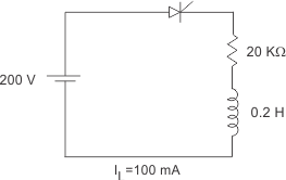
Power Electronics Latching current for an SCR inserted between a dc voltage source of 200 V and load is 100 mA. Compute the minimum rate of width pulse required to turn ON the SCR in case load consists of R = 20 Ω in series with L = 0.2 H. 300 µs. 150 µs. 100 µs. 200 µs. 300 µs. 150 µs. 100 µs. 200 µs. ANSWER DOWNLOAD EXAMIANS APP
Power Electronics Which one is most suitable power device for high frequency (>100 KHz) switching application? BJT. Power MOSFET. Schottky diode. Microwave transistor. BJT. Power MOSFET. Schottky diode. Microwave transistor. ANSWER DOWNLOAD EXAMIANS APP