Power Electronics After proper turn on of thyristor None of these gate signal is always present. gate signal should present but can be removed. gate signal must be removed. None of these gate signal is always present. gate signal should present but can be removed. gate signal must be removed. ANSWER DOWNLOAD EXAMIANS APP
Power Electronics Gate circuit or triggering circuit of a thyristor is high power circuit. lower power circuit. magnetic circuit. may be low power or high power circuit. high power circuit. lower power circuit. magnetic circuit. may be low power or high power circuit. ANSWER DOWNLOAD EXAMIANS APP
Power Electronics Under over voltage condition impedance offered by the voltage clamping device is moderate. high. low. infinity. moderate. high. low. infinity. ANSWER DOWNLOAD EXAMIANS APP
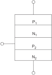
Power Electronics In a P1N1P2N2 thyristor which layer is less doped ? N2. P2. P1. N1. N2. P2. P1. N1. ANSWER DOWNLOAD EXAMIANS APP
Power Electronics A diac has ___________ semiconductor layers Four Three None of these Two Four Three None of these Two ANSWER DOWNLOAD EXAMIANS APP
Power Electronics Spread time is defined as the interval during which anode current rises from 90 % to its final value. anode voltage drops from 10 % of its initial value to zero. both (A) and (B). anode current rises from 10 % to 90 % of its final value. anode current rises from 90 % to its final value. anode voltage drops from 10 % of its initial value to zero. both (A) and (B). anode current rises from 10 % to 90 % of its final value. ANSWER DOWNLOAD EXAMIANS APP