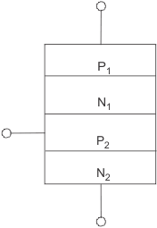
Power Electronics In a P1N1P2N2 thyristor which layer is less doped ? N2. N1. P2. P1. N2. N1. P2. P1. ANSWER DOWNLOAD EXAMIANS APP
Power Electronics Between the peak point and the valley point of UJT emitter characteristics we have ___________ region Saturation Negative resistance None of these Cut-off Saturation Negative resistance None of these Cut-off ANSWER DOWNLOAD EXAMIANS APP
Power Electronics Practical way of obtaining static voltage equalization in series connected SCRs is by the use of one resistor across the string. resistors of different values across each SCR. resistors of the same value across each SCR. one resistor in series with each SCR. one resistor across the string. resistors of different values across each SCR. resistors of the same value across each SCR. one resistor in series with each SCR. ANSWER DOWNLOAD EXAMIANS APP
Power Electronics Example of a voltage clamping device aluminium block. fast acting fuse. snubber circuit. metal oxide varistor. aluminium block. fast acting fuse. snubber circuit. metal oxide varistor. ANSWER DOWNLOAD EXAMIANS APP
Power Electronics Maximum power loss occurs during rise time. delay time. all. spread time. rise time. delay time. all. spread time. ANSWER DOWNLOAD EXAMIANS APP
Power Electronics The typical time of rising time lies between 10 - 20 µs. 1 - 4 µs. 90 - 100 µs. 40 - 60 µs. 10 - 20 µs. 1 - 4 µs. 90 - 100 µs. 40 - 60 µs. ANSWER DOWNLOAD EXAMIANS APP