Digital Electronics An AND gate can be imagined as transistors connected in series transistors connected in paralle switches connected in series switches connected in parallel transistors connected in series transistors connected in paralle switches connected in series switches connected in parallel ANSWER DOWNLOAD EXAMIANS APP
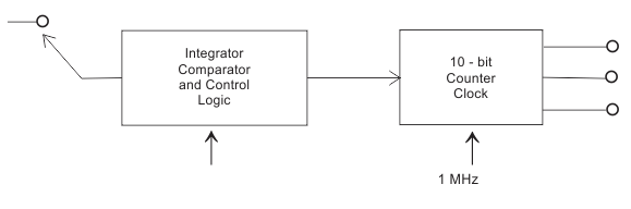
Digital Electronics The simplified block diagram of a 10-bit A/D converter of dual slope integrator type is shown in figure. The 10-bit counter at the output is clocked by a 1 Mhz clock. Assuming negligible timing overhead for the control logic, the maximum frequency of the analog signal that can be converted using this A/D converted is approximately . 1 KHz. 250 Hz. 2 KHz. 500 Hz. 1 KHz. 250 Hz. 2 KHz. 500 Hz. ANSWER DOWNLOAD EXAMIANS APP
Digital Electronics Why small bubble is given on the output of the NAND gate symbol ? Open collector output Output is inverted Tristate None of these Open collector output Output is inverted Tristate None of these ANSWER DOWNLOAD EXAMIANS APP
Digital Electronics 1s Complement of 11001010 is 11001011 11001001 00110101 00110111 11001011 11001001 00110101 00110111 ANSWER DOWNLOAD EXAMIANS APP
Digital Electronics At which the digital data can be applied to a a gate is known as ________ frequency. Operating Propagation Truth Run-time Operating Propagation Truth Run-time ANSWER DOWNLOAD EXAMIANS APP
Digital Electronics Number of 2 input multiplexers need to construct a 210 inputs multiplexer is _________ 129 9 32 1023 129 9 32 1023 ANSWER DOWNLOAD EXAMIANS APP